Friday 27 December 2013

0 Comments
Posted in Arrangement, Art, Business

PC Heat Monitor

The PC processor generates very high temperature during its operation which is dissipated by the large heat sink placed above the processor. If the heat sink assembly is not tight with the processor or the cooling fan is not working, PC enters into the Thermal shutdown mode and will not boot up. If the PC is not entering into thermal shutdown, the high temperature can destroy the processor. This simple circuit can be placed inside the PC to monitor the temperature near the processor. It gives warning beeps when the temperature near the heat sink increases abnormally. This helps to shutdown the PC immediately before it enters into Thermal shutdown.

Circuit Project: PC Heat Monitor Circuit 

The circuit uses a Piezo element (one used in Buzzer) as the heat sensor. The piezo crystals reorient when subjected to heat or mechanical stress and generates about one volt through the Direct piezoelectric property. IC1 is designed as a voltage sensor with both the inputs tied through the capacitor C1.The non inverting input is connected to the ground through R1 to keep the output low in the standby state. The inputs of IC1 are very sensitive and even a minute change in voltage level will change the output state.

Circuit Project: PC Heat Monitor Circuit

In the standby mode, both the inputs of IC1 are balanced so that output remains low. When the Piezo element accepts heat, it generates a minute voltage which will upset the input balance and output swings high. This triggers LED and Buzzer. Capacitor C2 gives a short lag before the buzzer beeps to avoid false triggering. Warning beep continues till the piezo element cools.

Note: Enclose the circuit inside the PC with the piezo element close to the heat sink of the processor. Adjust the distance between the piezo element and heat sink so as to keep the circuit standby in the normal condition. The piezo element can sense a 10 degree rise in temperature from a distance of 5 cms. Power to the circuit can be tapped from the 12 volt line of SMPS.
Thursday 26 December 2013

0 Comments
Posted in Arrangement, Art, Business

High Voltage DC Generator Circuit Diagram

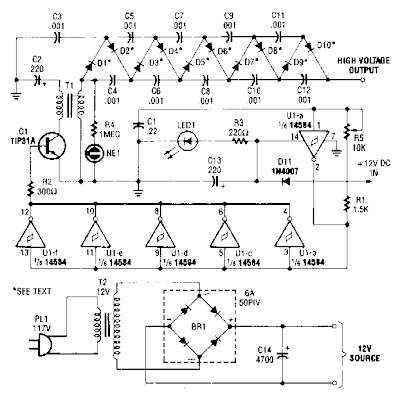
This circuit is fed from a 12-V de power supply. The input to the circuit is then amplified to provide a 10,000-Vdc output. The output of the up-converter is then fed into a 10 stage, high-voltage multiplier to produce an output of 10,000 Vdc.


High Voltage DC Generator Circuit Diagram

High Voltage DC Generator Circuit Diagram

Wednesday 25 December 2013

0 Comments
Posted in Arrangement, Art, Business

7805 Voltage Regulator Circuit

A voltage regulator is used to produce a constant linear output voltage. It’s generally used with AC to DC power supply. And also it can be used as well as a DC to DC voltage converter . To regulating low voltage, most used device is one single IC. 7805, 7812, 7905 etc. 78xx series are design for positive and 79xx series are for Negative voltage regulator.

7805 is a three terminal +5v voltage regulator IC from 78XX chips family. See 7805 pinout below. LM78XX series are from National Semiconductor. They are linear positive voltage regulator IC; used to produce a fixed linear stable output voltage.  National Semiconductor has also negative voltage regulator chips family, they indicate with LM 79XX. 78xx is used more than 79xx because negative voltage has a few usability purposes as we see.
I was previously posted a 5v regulated power supply circuit using 7805 IC, that circuit and this 7805 voltage regulator circuit is almost the same.


Circuit diagram of 7805 Voltage Regulator


Fig: 7805 Voltage Regulator Circuit


7805 pinout


7805 pinout, pin diagram
Fig: Pinout of 7805

Its output voltage is +5V DC that we need. You can supply any voltage in input; the output voltage will be always regulated +5V. But my recommendation is, don’t supply more than 18V or less than 8V in input. There used two capacitors in this voltage regulator circuit, they aren’t mandatory to use. But it will be best if you use them. They helped to produce a smooth regulated voltage at output. Use electrolyte capacitor instead of ceramic capacitor.

One limitation of 7805 I have found that is its output current 1A maximum. Otherwise it is a good voltage regulator if you are happy with 1A. But if   you need over 400mA current in output then you should use a Heat Sink with IC LM7805. Otherwise it may fall damage for overheating.

Tuesday 24 December 2013

0 Comments
Posted in Arrangement, Art, Business

Pre regulated High Voltage Power Supply Circuit Diagram

This Pre-regulated High Voltage Power Supply Circuit Diagram triacs selects the tap on main transformer Tl, which provides the proper, pre-regulated voltage to the secondary regulator. T2 and its associated components comprise the secondary regulator. The ADC 0804, IC1, digitizes a voltage-feedback signal from the secondary regulator`s output. 

 Pre-regulated High Voltage Power Supply Circuit Diagram

Pre-regulated High Voltage Power Supply Circuit Diagram


The MC1415 De-multiplexer, IC2, decodes the digitizer`s output. IC2, in turn, drives Tl`s opto-isolated triacs via the 74LS240 driver chip, IC3, and associated opto-isolators. Transformer T3 samples the circuit`s current output. The auxiliary, 12 V winding on Tl ensures noload starting. The combination of op amp IC5 and the inverting transistor, Ql, square this current signal. 

The output of Ql is the CLK signal, which triggers one-half of the one shot, IC4A, to begin the circuit`s AID conversion. The one shots` periods are set to time out within 1l2 cycle of the ac input. Upon completion of its AID conversion, ICl`s INTR output triggers the other half of the one shot, IC4B, which enables the converter`s data outputs. The rising edge of the CLK signal resets the one shot and latches the new conversion value into IC2. The latch, associated driver, and optoisolator trigger a selected triac according to the latest value of the voltage-feedback signal, V, . Keep enjoying dont forget click on share button .


Monday 23 December 2013

0 Comments
Posted in Arrangement, Art, Business

Mobile Car Stereo Player

Using a mobile phone while driving is dangerous. It is also against the law. However, you can use your mobile phone as a powerful music player with the help of a stereo power amplifier. This does away with the need of a sophisticated in-dash car music system. Most mobile phones have a music player that offers a number of features including preset/manual sound equalisers. They have standard 3.5mm stereo sockets that allow music to be played through standard stereo headphones/sound amplifiers. Nokia 2700 classic is an example.

Mobile Car Stereo Player Circuit Diagram

Circuit of mobile car stereo player

A car audio amplifier with 3.5mm socket can be designed and simply connected to the mobile phone output via a shielded cable with suitable connectors/jacks (readymade 3.5mm male-to-male connector cable is a good alternative). Fig. 1 shows the circuit of car stereo player. It is built around popular single-chip audio power amplifier TDA1554Q (IC1). The TDA1554Q is an integrated class-B power amplifier in a 17-lead single-in-line (SIL) plastic power package.

IC TDA1554Q contains four 11W identical amplifiers with differential input stages (two inverting and two non-inverting) and can be used for single-ended or bridge applications. The gain of each amplifier is fixed at 20 dB. Here it is configured as two 22W stereo bridge amplifiers. The amplifier is powered from the 12V car battery through RCA socket J2. Diode D1 protects against wrong-polarity connection. LED1 indicates the power status.

Stereo Jack :
3.5mm stereo socket and (b) 3.5mm

(a) 3.5mm stereo socket and (b) 3.5mm Stereo Jack

Connect stereo sound signal from the 3.5mm headset socket of the mobile phone to audio input socket J1. When you play the music from your mobile, IC1 amplifies the input. The output of IC1 is fed to speakers LS1 and LS2 fitted at a suitable place in your car. Electrolytic capacitor C5 connected between pin 4 of IC1 and GND improves the supply-voltage ripple rejection. Components R2 and C4 connected at mute/standby pin (pin 14) of IC1 eliminate the switch on/off plop. The circuit is quite compact. A good-quality heat-sink assembly is crucial for IC1. Fig. 2 shows the stereo socket and stereo jack.

Proposed enclosure
Proposed enclosure

Assemble the circuit on a general-purpose PCB and enclose in a suitable cabinet. Small dimensions of the power amplifier make it suitable for being enclosed in a plastic (ABS) case with vent holes. Signal input socket, speaker output terminals, on/off switch, indicator, fuse holder and power supply socket are best located on the front panel of the enclosure as shown in Fig. 3.

Source : http://www.ecircuitslab.com/2012/04/mobile-car-stereo-player.html

Sunday 22 December 2013

0 Comments
Posted in Arrangement, Art, Business

best cell phone jammer will stop working immediately

The over heat of best cell phone jammer should be timely dissipated.
Chinas mobile advertising does not scale, but it must embark on the road and internet advertising, but more business model remains to be explored. Several models of mobile media advertising. In China, mobile media advertising model can be divided into the following categories: the earliest provider of wireless advertising professional Focus wireless, using this model. There are two specific advertising: Point report, and direct report. Point report, through the identification of the users identity with the aid of technical means to fully tap the user attributes, automatically match the user properties to cater to user preferences ads to the users see on the page, different people see different ads precise The sentinel marketing. And get these best cell phone jammer directly from the supplier in the a shorter time.
Difficult to sell to a pack of cigarettes a woman, though she had the purchasing power, but she did not need, when you pass her cigarette advertising, is still spam. In other words, no will to produce spam, that is the wrong content delivery to the wrong object, although the advertising arrival rate, but not the demand, the result is still negative. SMS group sending, are examples. Win-win is the last word. The future of mobile advertising is first and foremost to be able to obtain permission from the customer, in other words, the ad itself is a value-added behavior for the audience, you can achieve a win-win of the advertisers and the audience will never users interfere. The inspection of some other wireless signals can be carried out by best cell phone jammer .
Type of mobile advertising is popular. Through a series of positioning and data analysis, cell text messaging information targeted to send to give advertising related to the user, for example, passengers waiting at the airport will often receive a discount ticket information. Business services, exhibition, hotel, shopping malls, automobile, FMCG, banking, real estate and other industries are beginning to Cell SMS platform to launch mobile advertising. "Mobile advertising mobile marketing is the next step." Communication University of China Vice-Chancellor Ding Junjie, "However, the main problems facing the mobile advertising is still lack a lot of professional standards, such as results-based monitoring of mobile advertising standards, the standard of the quotation system, advertising reach the standard of the cost of thousands of users and so on. And at the same time best cell phone jammer will stop working immediately.
Internet users are mainly concentrated in the eastern coastal areas and some inland provinces.

Saturday 21 December 2013

0 Comments
Posted in Arrangement, Art, Business

Build a 12 14 Volt 3A Anti RF Filtered Power supply Circuit Diagram

How to Build a 12-14 Volt 3A - Anti-RF Filtered Power supply Circuit Diagram. This is not easy but you can do it . This Anti-RF Filtered Power supply Circuit Diagram is dedicated for use with rf equipments like, linear amplifiers, transmitters, receivers, and in every application that clean an-noisy signal is required. 

The circuit is very simple and you can drive it with a 220V/18V/3A transformer at the pins 1and 2.The regulator used here is the LM350K and make sure you place a good heat-sink to it because it gets too hot if current gets near to 3A. 

 12-14 Volt 3A - Anti-RF Filtered Power supply Circuit Diagram

12-14 Volt 3A - Anti-RF Filtered Power supply Circuit Diagram


Parts list
R1 = 220 Ohm 1/4W
R2 = 1,8 KOhm 1/4W
R3 = 330 Ohm 1/4W
 P1 = 100 Ohm
C1,C2,C3 = 4.700uf/25V
C4 = 100pf ceramic
C6 = 100uf/25V electrolitic
D1..4 = 1N5400-4 or RAX GI 837U
F1 = 5A
IC1 = LM350K

For Data Sheet Contact with us here

Friday 20 December 2013

0 Comments
Posted in Arrangement, Art, Business

Loudspeaker Thump Remover Eliminator

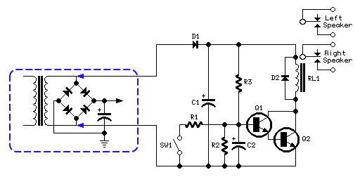
Some solid state power amplifiers make a loud thump when turned on or off. The thump you hear when you turn on or turn off your amplifier is caused by the sudden application or interruption in supply voltages to the amplifier output stages. To remove the thump, the output signal must be delayed (and thus the transient) until the output voltage will reach a safe level for the speakers.

In the circuit diagram, resistor R3 and capacitor C2 form an RC network timer. When voltage is applied to the circuit, R3 allows C2 to charge to about 1.2V. The transistors Q1 and Q2 are connected in a Darlington configuration and are then non-conducting until the charge across C2 does not exceed the sum of the base-emitter voltage of Q1 and Q2, i.e. 0.6V for each transistor for a total of 1.2V.

Loudspeaker Thump Remover Circuit Diagram

Once the voltage across C2 exceeds 1.2V, Q1 and Q2 immediately run into saturation, activating the relay RL1, which completes the circuit between the amplifier and speaker systems. The power supply circuit consists of a simple rectifier diode and a low value filter capacitor (D1 and C1). The ac voltage required is taken from the secondary winding of the transformer available in your amplifier.

In many cases, when dual supply is present and therefore the secondary winding is center tapped, the circuit can be connected across the central tap and one of the two outer leads of the winding or, on the contrary, across the whole winding. In the latter case, the available voltage will be twice the first case. This choice will affect also the coil operating voltage of the relay used.

You can choose a relay having a coil rated at 12V dc for a secondary winding ac voltage up to 15V; a 24V relay for an ac voltage up to 30V (or two SPST 12V relays wired in series, one for each channel). For higher ac voltages use a 48V relay or two SPST 24V relays wired in series. SW1 and R1 provide an optional mute facility: closing SW1 the Relay will go off and therefore the amplifier will be muted.

Notes:


  • After turn on, the relay will be activated with a delay of about 3 - 5 seconds. The delay time can vary by changing the values of R3 and/or C2.
  • If you do not want the mute function, SW1 and R1 can be omitted.
  • If two relays wired in series are employed, the added relay must have its own clamping diode connected across the coil.
  • When a voltage supply of about 48V is used, substitute BC337 transistors with BC546 types.


Thursday 19 December 2013

0 Comments
Posted in Arrangement, Art, Business

THIEF ALARM WITHOUT IC NE555


THIEF ALARM (WITHOUT IC NE555)
INDRODUCTION:-
This is the easiest way to make a thief alarm. If you know how to make an ordinary electric circuit, this circuit would be very simple than the other method.
MATERIALS REQUIRED:-
11)      Breadboard                                               1
22)      12v/230v Transformer                                1(2)
33)      Buzzer                                                        1
44)      LED                                                           4
55)      LDR(RESISTANCE IN DARKNESS       1
66)      Resistor 48 K Ohms                                   2
77)      Resistor 100 ohms                                      2
PROCEDURE:-  
Take the breadboard and connect the 12v/230v transformer to the pin numbers 5 and 10.connect the 100 ohms resistors to the pins 1b and 5b.Then connect one wire of the transformer directly to the resistors 48 k ohms leading to the +ve terminals of the buzzer and the LED. Then connect the next wire of the transformer to the LDR’s first terminal then connect the next terminal of the LDR to the –ve terminals of the buzzer and LED. Now switch off the light.When the intruder switches on his torch the
                                Circuit
    

Wednesday 18 December 2013

0 Comments
Posted in Arrangement, Art, Business

Simple 12 V Battery Charger Circuit Diagram

This 12 V Battery Charger Circuit Diagram is a high performance charger for gelled electrolyte lead-acid batteries. Charger quickly recharges battery and shuts off at full charge. Initially, charging current is limited to 2A. As the battery voltage rises, current to the battery decreases, and when the current has decreased to 150 mA, the charger switches to a lower float voltage preventing overcharge.

 12 V Battery Charger Circuit Diagram

12 V Battery Charger Circuit Diagram


When the start switch is pushed, the output of the charger goes to 14 V. As the battery approaches full charge, the charging current decreases and the output voltage is reduced from 14 V to about 12 5 V terminating the charging. Transistor Ql then lights the LED as a visual indication of full charge.

Tuesday 17 December 2013

0 Comments
Posted in Arrangement, Art, Business

Circuit Diagram of Photocell Power Supply MAX630

This Circuit Diagram of Photocell Power Supply (MAX630) delivers either 4.8 or 7.2 V regulated at 15 mA with a 3-V input from a bank of photocells. R1 should be 453 k? for a 7.2-V output and 274 k? for a 4.8-Vdc output. Regulator efficiency is around 70%. This should be considered when selecting suitable solar cells.

Circuit Diagram of Photocell Power Supply (MAX630)

Circuit Diagram of Photocell Power Supply (MAX630)

    Total Pageviews