Showing posts with label diagram. Show all posts

Thursday, 2 October 2014

0 Comments
Posted in Arrangement, Art, Business

Simple Triangle Square wave Oscillator Circuit Diagram

Simple triangle-square wave oscillator circuit diagram. In this circuit by making Rt variable it is possible to alter the operating frequency over a 100 to 1 range Versatile triangle/square wave oscillator has a possible frequency range of 0 Hz to 100 kHz.

Triangle Square wave Oscillator Circuit Diagram

Triangle Square wave Oscillator Circuit Diagram


Sourced By: circuitsdiagram-lab
0 Comments
Posted in Arrangement, Art, Business

Dual Regulated Power Supply Circuit Diagram

In this Dual Regulated Power Supply Circuit Diagram, the 7815 regulates the positive supply, and the 7915 regulates the negative supply. The transformer should have a primary rating of 240/220 volts for europe, or 120 volts for North America. The centre tapped secondary coil should be rated about 18 volts at 1 amp or higher, allowing for losses in the regulator. An application for this type of circuit would be for a small regulated bench power supply. 

 Dual Regulated Power Supply Circuit Diagram

Dual Regulated Power Supply Circuit Diagram

0 Comments
Posted in Arrangement, Art, Business

Stabilized Capacitance Buffer Circuit Diagram

This is a simplest Stabilized Capacitance Buffer Circuit Diagram. In this simple circuit using Ql and Q2 constitute a simple, high-speed FET input buffer. Ql functions as a source follower, with the Q2 current source load setting the drain-source channel current. The LT1010 buffer provides output drive capability for cables or whatever load is required. Normally, this open-loop configuration would be quite drifty because there is no de feedback. 

Stabilized Capacitance Buffer Circuit Diagram

Build a Stabilized Capacitance Buffer Circuit Diagram
The LTC1052 contributes this function to stabilize the circuit. It does this by comparing the filtered circuit output to a similarly filtered version of the input signal. The amplified difference between these signals is used to set Q2`s bias, and hence Ql `s channel current. Ql `s source line ensures that the gate never forward biases, and the 2000 pF capacitor at Al provides stable loop compensation. 
The rc network in Al`s output prevents it from seeing high-speed edges coupled through Q2`s collector-base junction. A2`s output is also fed back to the shield around Ql`s gate lead, bootstrapping the circuit`s effective in_put capacitance down to less than 1 pF.  

Sourced By : Circuitsstream
0 Comments
Posted in Arrangement, Art, Business

10 Watt Audio Power Amplifier Circuit Diagram

Build 10 Watt Audio Power Amplifier Circuit
10 Watt Audio Power Amplifier Circuit Diagram
10W PA.The 10 watts power amplifier circuit by transistor describe here is an audio amplifier with output power of 10W.Used as a low frequency class AB Amplifier. Transistor has high output current and very low distortion.This 10W audio amplifier circuit diagram using Transistor is good for small room or car audio system.This circuit is a general-purpose 10W audio amplifier for moderate-power PA or modulator use in an AM transmitter.
With higher voltages and a change in bias resistors,up to 30 W can be obtained. 

Sourced by: Circuitsstream
0 Comments
Posted in Arrangement, Art, Business

Build a Inexpensive Car Protection Unit Circuit Diagram

This is a simple Inexpensive car Protection Unit Circuit Diagram. This circuit to protect car stereo, etc from pilferage that costs less and requires no adjustments in the car but a good car cover. Place the circuit at your bedside and bring the two wires from the unit to the car (parked outside your home) and connect one wire-end to the cover and the other to the ground, with both wire-ends shorted by some weight such as a brick. So outwardly the mechanism is not visible.

Circuit of car protection unit with alarm

If someone tries to remove the cover, the alarm of the circuit starts sounding to alert you. The alarm can be switched off by resetting it using switch S1.

The car protection circuit comprises two timer ICs: one for the alarm circuit (see IC2 in Fig.1) and the other to indicate that the battery has taken over as the power source (see IC3 in Fig. 2). Normally, the protector operates off AC mains and the battery takes over only when mains fail. As the battery current is not high, the battery will last long.

As long as the two wires remain shorted, transistor T1 remains cut off. When shorting is removed, transistor T1 gets forward biased and its collector voltage drops to trigger IC2 and the piezobuzzer starts sounding.


battery-takeover indicator
 battery-takeover indicator

If mains fails, the battery-takeover indicator (shown in Fig. 2 and connected to points A, B and C in Fig. 1) immediately gets triggered at pin 2 of IC3. Its high output activates the battery-operation alarm for a couple of seconds. IC1 draws power from the battery to activate the protection unit.

After setting up the unit properly and shorting both the wires, press test switch S2. If there is no fault in the circuit, the alarm will sound. Now release test switch S2 and momentarily press reset switch S1 to switch off the alarm.


Sourced By:  EFY Author : M. Venkateswaran and T.E. Parthasarathy

Thursday, 9 January 2014

0 Comments
Posted in Arrangement, Art, Business

Build a Digital Electronic Lock Circuit Diagram

This Digital Electronic Lock Circuit Diagram shown below uses 4 common logic ICs to allow controlling a relay by entering a 4 digit number on a keypad. The first 4 outputs from the CD4017 decade counter (pins 3,2,4,7) are gated together with 4 digits from a keypad so that as the keys are depressed in the correct order, the counter will advance. As each correct key is pressed, a low level appears at the output of the dual NAND gate producing a high level at the output of the 8 input NAND at pin 13.

Read : Cheap Bicycle Alarm Schematics Circuit

Digital Electronic Lock Circuit Diagram

Digital Electronic Lock Circuit Diagram
 

The momentary high level from pin 13 activates a one shot circuit which applies an approximate 80 millisecond positive going pulse to the clock line (pin 14) of the decade counter which advances it one count on the rising edge.

Read : Emergency Light and Alarm Circuit Diagram

A second monostable, one shot circuit is used to generate an approximate 40 millisecond positive going pulse which is applied to the common point of the keypad so that the appropriate NAND gate will see two logic high levels when the correct key is pressed (one from the counter and the other from the key). The inverted clock pulse (negative going) at pin 12 of the 74C14 and the positive going keypad pulse at pin 6 are gated together using two diodes as an AND gate (shown in lower right corner).

Read : Burglar Alarm With Timed Shutoff Circuit Diagram

The output at the junction of the diodes will be positive in the event a wrong key is pressed and will reset the counter. When a correct key is pressed, outputs will be present from both monostable circuits (clock and keypad) causing the reset line to remain low and allowing the counter to advance. However, since the keypad pulse begins slightly before the clock, a 0.1uF capacitor is connected to the reset line to delay the reset until the inverted clock arrives.

Read : 5 Zone alarm Circuit Diagram

The values are not critical and various other timing schemes could be used but the clock signal should be slightly longer than the keypad pulse so that the clock signal can mask out the keypad and avoid resetting the counter in the event the clock pulse ends before the keypad pulse. The fifth output of the counter is on pin 10, so that after four correct key entries have been made, pin 10 will move to a high level and can be used to activate a relay, illuminate an LED, ect. At this point, the lock can be reset simply by pressing any key. The circuit can be extended with additional gates (one more CD4011) to accept up to a 8 digit code.

Read :  Alarm Control Keypad Circuit Diagram

The 4017 counting order is 3 2 4 7 10 1 5 6 9 11 so that the first 8 outputs are connected to the NAND gates and pin 9 would be used to drive the relay or light. The 4 additional NAND gate outputs would connect to the 4 remaining inputs of the CD4068 (pins 9,10,11,12). The circuit will operate from 3 to 12 volts on 4000 series CMOS but only 6 volts or less if 74HC parts are used. The circuit draws very little current (about 165 microamps) so it could be powered for several months on 4 AA batteries assuming only intermittent use of the relay.

Thursday, 26 December 2013

0 Comments
Posted in Arrangement, Art, Business

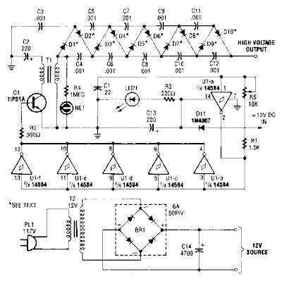
High Voltage DC Generator Circuit Diagram

This circuit is fed from a 12-V de power supply. The input to the circuit is then amplified to provide a 10,000-Vdc output. The output of the up-converter is then fed into a 10 stage, high-voltage multiplier to produce an output of 10,000 Vdc.


High Voltage DC Generator Circuit Diagram

High Voltage DC Generator Circuit Diagram

Tuesday, 24 December 2013

0 Comments
Posted in Arrangement, Art, Business

Pre regulated High Voltage Power Supply Circuit Diagram

This Pre-regulated High Voltage Power Supply Circuit Diagram triacs selects the tap on main transformer Tl, which provides the proper, pre-regulated voltage to the secondary regulator. T2 and its associated components comprise the secondary regulator. The ADC 0804, IC1, digitizes a voltage-feedback signal from the secondary regulator`s output. 

 Pre-regulated High Voltage Power Supply Circuit Diagram

Pre-regulated High Voltage Power Supply Circuit Diagram


The MC1415 De-multiplexer, IC2, decodes the digitizer`s output. IC2, in turn, drives Tl`s opto-isolated triacs via the 74LS240 driver chip, IC3, and associated opto-isolators. Transformer T3 samples the circuit`s current output. The auxiliary, 12 V winding on Tl ensures noload starting. The combination of op amp IC5 and the inverting transistor, Ql, square this current signal. 

The output of Ql is the CLK signal, which triggers one-half of the one shot, IC4A, to begin the circuit`s AID conversion. The one shots` periods are set to time out within 1l2 cycle of the ac input. Upon completion of its AID conversion, ICl`s INTR output triggers the other half of the one shot, IC4B, which enables the converter`s data outputs. The rising edge of the CLK signal resets the one shot and latches the new conversion value into IC2. The latch, associated driver, and optoisolator trigger a selected triac according to the latest value of the voltage-feedback signal, V, . Keep enjoying dont forget click on share button .


Saturday, 21 December 2013

0 Comments
Posted in Arrangement, Art, Business

Build a 12 14 Volt 3A Anti RF Filtered Power supply Circuit Diagram

How to Build a 12-14 Volt 3A - Anti-RF Filtered Power supply Circuit Diagram. This is not easy but you can do it . This Anti-RF Filtered Power supply Circuit Diagram is dedicated for use with rf equipments like, linear amplifiers, transmitters, receivers, and in every application that clean an-noisy signal is required. 

The circuit is very simple and you can drive it with a 220V/18V/3A transformer at the pins 1and 2.The regulator used here is the LM350K and make sure you place a good heat-sink to it because it gets too hot if current gets near to 3A. 

 12-14 Volt 3A - Anti-RF Filtered Power supply Circuit Diagram

12-14 Volt 3A - Anti-RF Filtered Power supply Circuit Diagram


Parts list
R1 = 220 Ohm 1/4W
R2 = 1,8 KOhm 1/4W
R3 = 330 Ohm 1/4W
 P1 = 100 Ohm
C1,C2,C3 = 4.700uf/25V
C4 = 100pf ceramic
C6 = 100uf/25V electrolitic
D1..4 = 1N5400-4 or RAX GI 837U
F1 = 5A
IC1 = LM350K

For Data Sheet Contact with us here

Wednesday, 18 December 2013

0 Comments
Posted in Arrangement, Art, Business

Simple 12 V Battery Charger Circuit Diagram

This 12 V Battery Charger Circuit Diagram is a high performance charger for gelled electrolyte lead-acid batteries. Charger quickly recharges battery and shuts off at full charge. Initially, charging current is limited to 2A. As the battery voltage rises, current to the battery decreases, and when the current has decreased to 150 mA, the charger switches to a lower float voltage preventing overcharge.

 12 V Battery Charger Circuit Diagram

12 V Battery Charger Circuit Diagram


When the start switch is pushed, the output of the charger goes to 14 V. As the battery approaches full charge, the charging current decreases and the output voltage is reduced from 14 V to about 12 5 V terminating the charging. Transistor Ql then lights the LED as a visual indication of full charge.

Tuesday, 17 December 2013

0 Comments
Posted in Arrangement, Art, Business

Circuit Diagram of Photocell Power Supply MAX630

This Circuit Diagram of Photocell Power Supply (MAX630) delivers either 4.8 or 7.2 V regulated at 15 mA with a 3-V input from a bank of photocells. R1 should be 453 k? for a 7.2-V output and 274 k? for a 4.8-Vdc output. Regulator efficiency is around 70%. This should be considered when selecting suitable solar cells.

Circuit Diagram of Photocell Power Supply (MAX630)

Circuit Diagram of Photocell Power Supply (MAX630)

Sunday, 6 October 2013

0 Comments
Posted in Arrangement, Art, Business

LONG RANGE FM TRANSMITTER ELECTRONIC DIAGRAM


LONG RANGE FM TRANSMITTER ELECTRONIC DIAGRAM

This circuit works optimally by adding RF amplifier and antenna. Here is the schematic diagram :

Parts list :


  •     Diode D1 : BB109
  •     Resistor R1 : 10k ohm
  •     Resistor R2 : 100k ohm
  •     Resistor R3 : 180k ohm
  •     Resistor R4 : 4K7
  •     Resistor R5 : 15k ohm
  •     Resistor R6 : 68 ohm
  •     Resistor R7 : 470 ohm
  •     Resistor R8 : 39k ohm
  •     Resistor R9 : 10 ohm
  •     VR1 : 47k ohm
  •     VR2 : 22 ohm
  •     Capacitor C1-C3, C8 : 0.1 uF
  •     Capacitor C4 : 4.7 pF
  •     Capacitor C6 : 0.01 uF
  •     Capacitor C7 : 5.6 nF
  •     Capacitor C9 : 100 pF
  •     Transistor T1: BF494
  •     Transistor T2:2N3866
  •     Trimmer VC1-VC2 : 50p
  •     L1 : 4 round 20 cables SWG in plastic with 8mm diameter
  •     L2 : 2 round 24 cables SWG
  •     L3 : 7 round 24 cables SWG in plactic with 4mm diameter
  •     L4 : 7 round 24 cables SWG in ferrid bead


Saturday, 28 September 2013

0 Comments
Posted in Arrangement, Art, Business

Diagram Push Bike Light


This design was primarily intended to allow automatic switch-on of push-bike lights when it gets dark. Obviously, it can be used for any other purpose involving one or more lamps to be switched on and off depending of light intensity. Power can be supplied by any type of battery suitable to be fitted in your bike and having a voltage in the 3 to 6 Volts range. The Photo resistor R1 should be fitted into the box containing the complete circuit, but a hole should be made in a convenient side of the box to allow the light hitting the sensor. Trim R2 until the desired switching threshold is reached. The setup will require some experimenting, but it should not be difficult.

Push-Bike Light Circuit DiagramParts:

R1_____________Photo resistor (any type)
R2______________22K 1/2W Trimmer Cermet or Carbon type
R3_______________1K 1/4W Resistor
R4_______________2K7 1/4W Resistor
R5_____________330R 1/4W Resistor (See Notes)
R6_______________1R5 1W Resistor (See Notes)
D1____________1N4148 75V 150mA Diode
Q1_____________BC547 45V 200mA NPN Transistor
Q2_____________BD438 45V 4A PNP Transistor
LP1____________Filament Lamp(s) (See Notes)
SW1_____________SPST Toggle or Slider Switch
B1______________6V or 3V Battery (See Notes)

Notes:
  • In this circuit, the maximum current and voltage delivered to the lamp(s) are limited mainly by R6 (that cant be omitted if a clean and reliable switching is expected). Therefore, the Ohms Law must be used to calculate the best voltage and current values of the bulbs.
  • For example: at 6V supply, one or more 6V bulbs having a total current drawing of 500mA can be used, but for a total current drawing of 1A, 4.5V bulbs must be chosen, as the voltage drop across R6 will become 1.5V. In this case, R6 should be a 2W type.
  • At 3V supply, R6 value can be lowered to 1 or 0.5 Ohm and the operating voltage of the bulbs should be chosen accordingly, by applying the Ohms Law.
  • Example: Supply voltage = 3V, R6 = 1R, total current drawing 600mA. Choose 2.2V bulbs as the voltage drop caused by R6 will be 0.6V.
  • At 3V supply, R5 value must be changed to 100R.
  • Stand-by current is less than 500µA, provided R2 value after trimming is set at about 5K or higher: therefore, the power switch SW1 can be omitted. If R2 value is set below 5K the stand-by current will increase substantially.

Friday, 27 September 2013

0 Comments
Posted in Arrangement, Art, Business

A Simple Tan Timer Circuit Diagram

Six timing positions suited to different skin types, Timing affected by sunlight intensity

This timer was designed for people wanting to get tanned but at the same time wishing to avoid an excessive exposure to sunlight. A Rotary Switch sets the timer according to six classified Photo-types (see table). A Photo resistor extends the preset time value according to sunlight brightness (see table). When preset time ends, the beeper emits an intermittent signal and, to stop it, a complete switch-off of the circuit via SW2 is necessary.

Circuit diagram:

A Simple Tan Timer Circuit Diagram

A Simple Tan Timer Circuit Diagram

Parts:

R1 = 47K - 1/4W Resistor
R2 = 1M - 1/4W Resistor
R3 = 120K - 1/4W Resistors
R4 = Photo resistor (any type)
R5 = 120K - 1/4W Resistors
C1 = 10µF - 25V Electrolytic Capacitors
C2 = 220nF - 63V Polyester Capacitor
C3 = 10µF - 25V Electrolytic Capacitors
D1 = 1N4148 - 75V 150mA Diodes
D2 = 1N4148 - 75V 150mA Diodes
Q1 = BC337 - 45V 800mA NPN Transistor
B1 = 3V Battery (two 1.5V AA or AAA cells in series)
IC1 = 4060 - 14 stage ripple counter and oscillator IC
IC2 = 4017 - Decade counter with 10 decoded outputs IC
SW1 = 2 poles 6 ways Rotary Switch (see notes)
SW2 = SPST Slider Switch
BZ1 = Piezo sounder (incorporating 3KHz oscillator)


Photo-type

Features

Exposure time

I & children

Light-eyed, red-haired, light complexion, freckly

20 to 33 minutes

II

Light-eyed, fair-haired, light complexion

28 to 47 minutes

III

Light or brown-eyed, fair or brown-haired, light or slightly dark complexion

40 to 67 minutes

IV

Dark-eyed, brown-haired, dark complexion

52 to 87 minutes

V

Dark-eyed, dark-haired, olive complexion

88 to 147 minutes

VI

The darkest of all

136 to 227 minutes

Note that pregnant women belong to Photo-type I

Notes:

  • Needing only one time set suitable for your own skin type, the rotary switch can be replaced by hard-wired links.
  • A DIP-Switch can be used in place of the rotary type. Please pay attention to use only one switch at a time when the device is off, or the ICs could be damaged.

Source : www.redcircuits.com

Monday, 23 September 2013

0 Comments
Posted in Arrangement, Art, Business

AUTO RETRY fOR MAX1637 STEP DOWN CONTROLLER ELECTRONIC DIAGRAM


AUTO RETRY fOR MAX1637 STEP-DOWN CONTROLLER ELECTRONIC DIAGRAM

On microprocessor supervisor (IC1), an internal power-fail comparator and manual-reset circuitry (MR) is included. IC1s PFI input will detect when Vout(1.8V) is above the internal reference voltage (1.25V). Active-low RESET and active-low SHDN go high after a timeout delay of 140ms, re-enabling IC2. The other way to re-enabling IC2 is when the supply voltage is first switched on : the 3.5V rail stabilizes after 140ms will cause active-low RST to go high and activate IC2.The active-low PFO output produces a pulse using the internal 60k pull-up resistor and external 0.1 uF capacitor if Vout falls below 1.25V (due to a short circuit, for instance).

Sunday, 22 September 2013

0 Comments
Posted in Arrangement, Art, Business

1995 Ford Probe Wiring Diagram

1995 Ford Probe Wiring Diagram


The Part of 1995 Ford Probe Wiring Diagram: interior fuse panel, power relay, splice, connector, engine
compartment, fuse box, power distribution, solenoid valve, automatic transaxle, solid state, powertrain ctrl module, fuel pump module, shutoff switch

Saturday, 21 September 2013

0 Comments
Posted in Arrangement, Art, Business

Fuse Box BMW Cibie CSR Diagram

Fuse Box BMW Cibie CSR Diagram - Here are new post for Fuse Box BMW Cibie CSR Diagram.

Fuse Box BMW Cibie CSR Diagram


Fuse Box BMW Cibie CSR Diagram

Fuse Panel Layout Diagram Parts: high beam relay, low beam relay, auxiliary fan, turn signal, windshield wiper/washer, intensive cleaner, brake light, cruise control, horn, engine electrical equipment, back up light, fuel pump, check control, instrument cluster, on board computer, heater blower, back up light, outside power mirror, mirror heating, air conditioner, power seat memory, rear window defogger, interior light, glove box, memory, rechargable flash light, hazard warning light, engine compartment light, license plate light, power antenna, parked car heater, fog light.

Friday, 20 September 2013

0 Comments
Posted in Arrangement, Art, Business

Fuse Box BMW R1150GS Diagram

Fuse Box BMW R1150GS Diagram - Here are new post for Fuse Box BMW R1150GS Diagram.

Fuse Box BMW R1150GS Diagram


Fuse Box BMW R1150GS Diagram

Fuse Panel Layout Diagram Parts: flasher unit, dial needle damping, coding plug motronic, starter relay, load relief relay, horn relay, fuel pump relay, motronic relay, ABS warning system.

Monday, 12 August 2013

0 Comments
Posted in Arrangement, Art, Business

Build a Voice Scrambler or Descrambler Circuit Diagram

This Voice Scrambler or De-scrambler Circuit Diagram uses an NE602 as an inversion mixer. U2 is set to run at about 2.5 to 3.5 kHz. U3 drives a loudspeaker. Because speech inversion scrambling is its own inverse, the circuit will also descramble . 

Voice Scrambler or Descrambler Circuit Diagram

Voice Scrambler or Descrambler Circuit Diagram

Tuesday, 6 August 2013

0 Comments
Posted in Arrangement, Art, Business

Precision Full Wave Ac Dc Converter Circuit Diagram

A dc level is produced that corresponds to the ac input rms value (if sine wave), -i set the gain of IC2 to 1.11. This factor is the average-to-rms conversion factor. IC1 and IC2 act as a full-wave rectifier circuit, with Dl and D2. 

Precision Full-Wave Ac/Dc Converter Circuit Diagram


Precision Full-Wave Ac/Dc Converter Circuit Diagram

    Total Pageviews