Showing posts with label simple. Show all posts

Thursday, 2 October 2014

0 Comments
Posted in Arrangement, Art, Business

Simple Triangle Square wave Oscillator Circuit Diagram

Simple triangle-square wave oscillator circuit diagram. In this circuit by making Rt variable it is possible to alter the operating frequency over a 100 to 1 range Versatile triangle/square wave oscillator has a possible frequency range of 0 Hz to 100 kHz.

Triangle Square wave Oscillator Circuit Diagram

Triangle Square wave Oscillator Circuit Diagram


Sourced By: circuitsdiagram-lab
0 Comments
Posted in Arrangement, Art, Business

Simple High Power Triac Dimmable LED Driver

A 20 Watt Triac dimmable LED driver. This is basically a current controlled step-down switching power supply. The circuit is powered directly from mains so be careful with this one.

Wednesday, 18 December 2013

0 Comments
Posted in Arrangement, Art, Business

Simple 12 V Battery Charger Circuit Diagram

This 12 V Battery Charger Circuit Diagram is a high performance charger for gelled electrolyte lead-acid batteries. Charger quickly recharges battery and shuts off at full charge. Initially, charging current is limited to 2A. As the battery voltage rises, current to the battery decreases, and when the current has decreased to 150 mA, the charger switches to a lower float voltage preventing overcharge.

 12 V Battery Charger Circuit Diagram

12 V Battery Charger Circuit Diagram


When the start switch is pushed, the output of the charger goes to 14 V. As the battery approaches full charge, the charging current decreases and the output voltage is reduced from 14 V to about 12 5 V terminating the charging. Transistor Ql then lights the LED as a visual indication of full charge.

Tuesday, 1 October 2013

0 Comments
Posted in Arrangement, Art, Business

Ultra Simple Microphone Preamplifier

This little project came about as a result of a design job for a client. One of the items needed was a mic preamp, and the project didnt warrant a design such as the P66 preamp, since it is intended for basic PA only. Since mic preamps are needed by people for all manner of projects, this little board may be just whats needed for interfacing a balanced microphone with PC sound cards or other gear. Unlike most of my boards, this one is double-sided. I normally avoid double-sided PCBs for projects because rework by those inexperienced in working with them will almost certainly damage the board beyond repair. I consider this not to be an issue with this preamp, because it is so simple. It is extremely difficult to make a mistake because of the simplicity.

Ultra-Simple Microphone PreamplifierPhoto of Completed Board

As you can see, the board uses a PCB mounted XLR connector and pot, so is a complete mic preamp, ready to go. Feel free to ignore the terminals marked SW1 (centred between the two electrolytic supply caps), as they are specific to my clients needs and are not useful for most applications. The original use was to use them for a push-button switch that activated an audio switch via a PIC micro-controller. They are not shown on the schematic.

The DC, GND and output terminals may be hard wired to the board, you may use PCB pins or a 10-way IDC (Insulation Displacement Connector) and ribbon cable. Power can be anything between +/-9V and +/-18V with an NE5532 opamp. The mic input is electronically balanced, and noise is quite low if you use the suggested opamp. Gain range is from about 12dB to 37dB as shown. It can be increased by reducing the value of R6, but this should not be necessary. Because anti-log pots are not available, the gain control is not especially linear, but unfortunately in this respect there is almost no alternative and the same problem occurs with all mic preamps using a similar variable gain control system.

Ultra-Simple Microphone Preamplifier circuit diagramFigure 1 - Preamp Schematic

The circuit is quite conventional, and if 1% metal film resistors are used throughout it will have at least 40dB of common mode rejection with worst-case values. The input capacitors give a low frequency rolloff of -3dB at about 104Hz. If better low frequency response is required, these caps may be increased to 4.7uF or 10uF bipolar electrolytics. These will give response to well below 10Hz if you think youll ever need to go that low.

The project PCB measures 77 x 24mm, and the mounting centers for the pot and XLR connector are spaced at 57mm. If preferred, a traditional chassis mounted female XLR can be used, and wired to the board with heavy tinned copper wire. The PCB pads for the connector are in the correct order for a female chassis mount socket mounted with the "Push" tab at the top.

Friday, 27 September 2013

0 Comments
Posted in Arrangement, Art, Business

A Simple Tan Timer Circuit Diagram

Six timing positions suited to different skin types, Timing affected by sunlight intensity

This timer was designed for people wanting to get tanned but at the same time wishing to avoid an excessive exposure to sunlight. A Rotary Switch sets the timer according to six classified Photo-types (see table). A Photo resistor extends the preset time value according to sunlight brightness (see table). When preset time ends, the beeper emits an intermittent signal and, to stop it, a complete switch-off of the circuit via SW2 is necessary.

Circuit diagram:

A Simple Tan Timer Circuit Diagram

A Simple Tan Timer Circuit Diagram

Parts:

R1 = 47K - 1/4W Resistor
R2 = 1M - 1/4W Resistor
R3 = 120K - 1/4W Resistors
R4 = Photo resistor (any type)
R5 = 120K - 1/4W Resistors
C1 = 10µF - 25V Electrolytic Capacitors
C2 = 220nF - 63V Polyester Capacitor
C3 = 10µF - 25V Electrolytic Capacitors
D1 = 1N4148 - 75V 150mA Diodes
D2 = 1N4148 - 75V 150mA Diodes
Q1 = BC337 - 45V 800mA NPN Transistor
B1 = 3V Battery (two 1.5V AA or AAA cells in series)
IC1 = 4060 - 14 stage ripple counter and oscillator IC
IC2 = 4017 - Decade counter with 10 decoded outputs IC
SW1 = 2 poles 6 ways Rotary Switch (see notes)
SW2 = SPST Slider Switch
BZ1 = Piezo sounder (incorporating 3KHz oscillator)


Photo-type

Features

Exposure time

I & children

Light-eyed, red-haired, light complexion, freckly

20 to 33 minutes

II

Light-eyed, fair-haired, light complexion

28 to 47 minutes

III

Light or brown-eyed, fair or brown-haired, light or slightly dark complexion

40 to 67 minutes

IV

Dark-eyed, brown-haired, dark complexion

52 to 87 minutes

V

Dark-eyed, dark-haired, olive complexion

88 to 147 minutes

VI

The darkest of all

136 to 227 minutes

Note that pregnant women belong to Photo-type I

Notes:

  • Needing only one time set suitable for your own skin type, the rotary switch can be replaced by hard-wired links.
  • A DIP-Switch can be used in place of the rotary type. Please pay attention to use only one switch at a time when the device is off, or the ICs could be damaged.

Source : www.redcircuits.com

Wednesday, 11 September 2013

0 Comments
Posted in Arrangement, Art, Business

Simple Voltage to Current Converter Drives White LEDs

You sometimes need to drive a white LED from one 1.5V battery. Unfortunately, the forward voltage of a white LED is 3 to 4V. So, you would need a dc/dc converter to drive the LED from one battery. Using the simple circuit in Figure 1, you can drive one white LED or two series-connected green LEDs, using only a few components. The circuit is a voltage-to-current converter, which converts the battery voltage to a current that passes through the LED.

You can adjust this current and, thus, the brightness of the LED, by varying resistor R3. If you turn on switch S1, resistor R2 feeds base current to transistor Q2. Q2 turns on, and its collector current, via R3, turns on Q1. Now, the current through inductor L1 increases. The slope of the increase is a function of the value of L1 and the battery voltage. The current through L1 increases until it reaches a maximum value, which depends on the gain of Q1. Because the value of R3 sets the base current drawn from Q1, Q1s collector current is also limited.

White LEDs Circuit Diagram

White LEDs Circuit Diagram


Once the current through L1 reaches its maximum value, the slope of the current through L1 changes. At that instant, the voltage on L1 switches to a negative polarity forced by the changed slope. This negative voltage traverses capacitor C1 and turns off Q2, which in turn turns off Q1. The negative voltage on L1 increases until it reaches the forward voltage of the LED. The peak current through inductor L1 now flows through the LED and decreases to zero. Now, Q2 switches on again, via the current through R2, and the cycle starts again.

By adjusting resistor R3, you can set the peak current through L1 and the peak current through the LED. The brightness of an LED is a linear function of the current through the LED. So, adjusting the value of R3 also adjusts the brightness of the LED.

It doesnt matter which LED you use; the forward voltage on the LED always increases until the peak current through L1 flows through the LED. Different forward voltages of the LEDs yield different on-times (duty cycles) but the same peak current through the LED. With the values shown in Figure 1, the circuit oscillates at a frequency of approximately 30 kHz and delivers a 20-mA peak current through the LED.

The duty cycle depends on the ratio of the battery voltage to the forward voltage of the LED. One advantage of this circuit is that it requires no series-limiting resistor for the LED. The peak current through the LED is a function of the value of R3 and the gain of Q1.[via]

Tuesday, 10 September 2013

0 Comments
Posted in Arrangement, Art, Business

Simple Wireless TRIAC Dimmer

This project was used as a wireless light dimmer, but in principle can be used to dim resistive loads and wirelessly turn on/off loads. The current code includes a routine to dim a light bulb in a “heartbeat” pattern, with the heartbeat frequency remotely adjustable.


The top left of the schematic shows the wall outlet (US 120VAC) being stepped down with a small transformer, then full rectified and regulated. This powers the entire board from the wall. The top right shows a microcontroller, ATmega48, its programming header, and a UART connection to the microcontroller (for debugging). The bottom right shows the XBee and its basic voltage regulation (it’s 3.3V), as well as an LED that indicates when the XBee is connected.

Wednesday, 14 August 2013

0 Comments
Posted in Arrangement, Art, Business

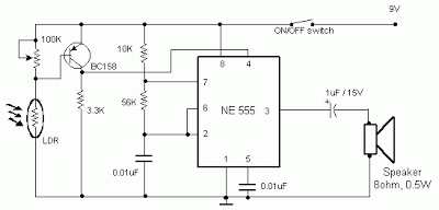
Simple Light Sensor Alarm circuit with NE555

Occurring this circuit sent out an alarm when its LDR sensor is exposed to light by sun or lamp. A 555 stable multivariate was used here which sent signal a tone of about 1kHz upon detecting light.The sensor when exposed by light completes the circuit and makes the 555 oscillate at about 1kHz with transistor to drive current.

The sensor is also shown in the circuit diagram. It has to placed making an angle of about 30 – 45 degrees to the ground.

 Light Sensor Alarm circuit with NE555
 Sensitivity can be adjust with P1.
 This makes the sun light to flow through it to the ground and prevents the alarm from going on due to the stored light on the sensor

Saturday, 3 August 2013

0 Comments
Posted in Arrangement, Art, Business

Simple Audio Filter Analyzer Circuit

When this circuit is connected to a filter and an oscilloscope, the scope displays the filter`s frequency response. A frequency that sweeps from low to high is applied to a filter. An oscilloscope is triggered by* the start of the sweep and ends its trace at the highest frequency of the sweep. The filter output goes to the vertical amplifier of the oscilloscope. Using bandpass filters as an example, as the bandpass frequency is approached, reached, and passed, the scope follows the peaking output and draws the response curve. A neat effect! The 566 VCO (Ul) produces a VLF triangle wave to frequency modulate the next stage. 

 Audio Filter Analyzer Circuit Diagram

Audio Filter Analyzer Circuit

It also produces a square wave to externally trigger the scope. Op amp U2 (a 741 unit) optimizes the amplitude and the dc component. Another VCO (U3) produces the actual sweeping triangle wave. Its frequency is selectable via SI. Op amp U4 (another 741 op amp) is set up as a bandpass filter and has been included as an example filter. Finally, diode D1 chops off the bottom half of the output, and leaves a nice bell curve. lb set up and operate, power-up the circuit and scope. Set the scope`s TIME/CM to 50 ms/cm. Set the VOLTS/CM control to 2 V. Attach a probe from the circuit`s trigger to the scope`s external trigger input. Set the triggering mode to normal, external. Attach a probe from the vertical amplifier to TP1. You`ll see a diagonal line that runs across the CRT. Input coupling should be set to dc. Adjust the triggering level until the diagonal runs from the upper left to the lower right of the CRT to ensure a displayed sweep from low to high. Now, disconnect the probe from TP1 and attach it to the filter output past the diode.

Sunday, 19 May 2013

0 Comments
Posted in Arrangement, Art, Business

Simple electronics Code Lock System

SIMPLE ELECTRONIC
CODE LOCK
The circuit diagram of a simple electronic
code lock is shown in figure.
A 9-digit code number is used
to operate the code lock.
When power supply to the circuit is
turned on, a positive pulse is applied to
the RESET pin (pin 15) through capacitor
C1. Thus, the first output terminal
Q1 (pin 3) of the decade counter IC (CD
4017) will be high and all other outputs
(Q2 to Q10) will be low. To shift the high
state from Q1 to Q2, a positive pulse must
be applied at the clock input terminal (pin
14) of IC1. This is possible only by pressing
the push-to-on switch S1 momentarily.
On pressing switch S1, the high state
shifts from Q1 to Q2.


Now, to change the high state from
Q2 to Q3, apply another positive pulse at
pin 14, which is possible only by pressing
switch S2. Similarly, the high state can
be shifted up to the tenth output (Q10)
by pressing the switches S1 through S9
sequentially in that order. When Q10 (pin
11) is high, transistor T1 conducts and
energises relay RL1. The relay can be
used to switch ‘on’ power to any electrical
appliance.
Diodes D1 through D9 are provided
to prevent damage/malfunctioning of the
IC when two switches corresponding to
‘high’ and ‘low’ output terminals are
pressed simultaneously. Capacitor C2 and
resistor R3 are provided to prevent noise
during switching action.
Switch S10 is used to reset the
circuit manually.

Switches S1 to S10
can be mounted on a keyboard panel,
and any number or letter can be used to
mark them. Switch S10 is also placed
together with other switches so that any
stranger trying to operate the lock frequently
presses the switch S10, thereby
resetting the circuit many times. Thus,
he is never able to turn the relay ‘on’. If
necessary, two or three switches can
be connected in parallel with S10 and
placed on the keyboard panel for more
safety.
A 12V power supply is used for the
circuit. The circuit is very simple and can
be easily assembled on a general-purpose
PCB. The code number can be easily
changed by changing the connections to
switches (S1 to S9).

Thursday, 2 May 2013

0 Comments
Posted in Arrangement, Art, Business

Simple Multiple Continuity Tester

http://s.eeweb.com/members/circuit_projects/blog/2012/01/21/circuit-continuity-tester-using-op-amps-1327172100.gifThe continuity tester is a handy adjunct to an ohmmeter. The unit or component whose continuity is to be checked is connected between terminals E1 and E2 (which may be probes or croc clips). The test current then flowing through the unit/component on test causes a potential drop across resistor R2, which is applied to the non-inverting input of buffer IC2. The output of the op amp is applied to transistor T1, in the emitter circuit of which there are a number of parallel-connected light-emitting diodes. Each LED is in series with a zener diodes and a resistor. The zener diodes have dissimilar zener voltages as shown in the diagram. When the drop across R2 exceeds the sum of base-emitter voltage of T1, a zener voltage, and the threshold voltage of the LED in series with that zener diode, the relevant LED lights. which resistance value of the unit/component on test a particular LED lights. Bear in mind, however, that these values depend to some extent on the type of LED, and also that the zener voltages are subject to tolerances. Serious deviations may be corrected by the addition of a standard diode or a Schottky diode. It is also possible to add branches to individual requirements, or to use a bar display instead of LEDs. It is important that the op amp used has a rail-to-rail output since the input voltages as well as the output may rise to the peak supply voltage. This requirement is met by the MAX4322 as used in the prototype.

Monday, 29 April 2013

0 Comments
Posted in Arrangement, Art, Business

Simple Low Drop 5V Regulator

A 4-cell pack is a convenient, popular battery size. Alkaline manganese batteries are sold in retail stores in packs of four, which usually provide sufficient energy to keep battery replacement frequency at a reasonable level. Generating 5 V from four batteries is, however, a bit tricky. A fresh set of four batteries has a terminal voltage of 6.4 V, but at the end of their life, this voltage is down to 3.2 V. Therefore, the voltage needs to be stepped up or down, depending on the state of the batteries. A flyback topology with a costly, custom designed transformer could be used, but the circuit in the diagram gets around the problem by using a flying capacitor together with a second inductor.

Circuit diagram:

The circuit also isolates the input from the output, allowing the output to go to 0 V during shutdown. The circuit can be divided conceptually into boost and buck sections. Inductor L1 and switch IC1 comprise the boost or step-up section, and inductor L2, diode D1 and capacitor C3 form the buck or step-down section. Capacitor C2 is charged to the input voltage, Vin, and acts as a level shift between the two sections. The switch toggles between ground and Vin+Vout , while the junction of L2, C2 and D1 toggles between –Vin and Vout +Vd1. Efficiency is directly related to the quality of the capacitors and inductors used.

Better quality capacitors are more expensive. Better quality inductors need not cost more, but normally take up more space. The Sanyo capacitors used in the prototype (C1–C3) specify a maximum ESR (effective series resistance) of 0.045 ½ and a maximum ripple current rating of 2.1 A. The inductors used specify a maximum DCR (direct current resistance) of 0.058 ½. Worst-case r.m.s. current through capacitor C2 occurs at minimum input voltage, that is, 400 mA at full load with an input voltage of 3 V. 

Friday, 12 April 2013

0 Comments
Posted in Arrangement, Art, Business

Simple Light Sensor Alarm circuit with NE555

Occurring this circuit despatched out an alarm when its LDR sensor is exposed to gentle by way of solar or lamp. A 555 steady multivariate used to be used here which sent sign a tone of about 1kHz upon detecting mild.The sensor when uncovered by mild fulls the circuit and makes the 555 oscillate at about 1kHz with transistor to pressure current.

The sensor can be shown within the circuit diagram. It has to placed making an angle of about 30 – forty five degrees to the bottom.

 Sensitivity will additionally be regulate with P1.
 This makes the solar gentle to drift via it to the bottom and stops the alarm from happening as a outcome of the saved mild on the sensor

Tuesday, 9 April 2013

0 Comments
Posted in Arrangement, Art, Business

Simple Peak Indicator

A simple circuit, peak indicator of tops of musical signal. Each time where the level of signal exceeds the level + 4dB, turns on led D1. It is useful in each channel of console of sound, in final amplifiers or in that other application, to we needed. With the prices of circuit, the indicate begins with levels above + 4 dB (1.25V rms). For adaptation in different levels of signal, we can use a trimmer, before capacitor C1.

Peak Indicator Circuit Diagram :
PeakIndicator Circuit diagram

Parts:

R1 = 10K
R2 = 1.2K
R3 = 220K
R4 = 4.7K
R5 = 4.7K
C1 = 47uF-25V
C2 = 2.2uF-25V
Q1 = BC550C
Q2 = BC550C
D1 = Red LED

Notes:
  • It can be assembled on a general purpose PCB.
  • It can be powered from a 12V-15V regulated power supply.
Source : www.ecircuitslab.com/2011/05/simple-peak-indicator.html

Monday, 8 April 2013

0 Comments
Posted in Arrangement, Art, Business

Simple Steam Whistle

This circuit consists of six square wave oscillators. Square waves are made up of a large number of harmonics. If six square waves with different frequencies are added together, the result will be a signal with a very large number of frequencies. When you listen to the result you’ll find that it is very similar to a steam whistle. The circuit should be useful in modelling or even in a sound studio.
Circuit diagram :
Simple Steam Whistle-Circuit Diagram
Simple Steam Whistle Circuit Diagram

This circuit uses only two ICs. The first IC, a 40106, contains six Schmitt triggers, which are all configured as oscillators. Different frequencies are generated by the use of different feedback resistors. The output signals from the Schmitt triggers are mixed via resistors. The resulting signal is amplified by IC2, an LM386. This IC can deliver about 1 W of audio power, which should be sufficient for most applications. If you leave out R13 and all components after P1, the output can then be connected to a more powerful amplifier. In this way a truly deafening steam whistle can be created. The ‘frequency’ of the signal can be adjusted with P2, and P1 controls the volume.


Streampowers

    Total Pageviews